-
Established in 2020, Draking Semiconductor was jointly founded by the core team of a leading Chinese semiconductor listed company and core technical personnel from world-leading companies.

-
-
The company has assembled a strong R&D and process team, continuously improving in aspects such as diamond powder material selection and dispersion, electroplating technology, precision processing technology, and adhesive formulation.

-
Draking Semiconductor Technology can perform dicing on chips such as IGBT chips, SiC chips, lithium tantalate/lithium niobate chips, integrated circuit IC chips, and double-bonded chips, as well as on packages such as QFN and DFN, and ceramic and glass substrates.

-
-


Product Center
Wafer Dicing Services
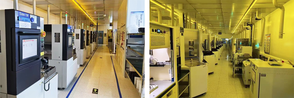
OverviewDraking Semiconductor Technology started its chip packaging lapping and scribing business in 2023. The company has an 800-square-meter class 1000 cleanroom for lapping and scribing operations, equipped with a professional application technology team. Through professional teams, equipment, and consumables, it provides lapping and scribing processing services for packaging customers and IC design customers. Currently, it has established mature processes for wafer front-side film lamination, back-side thinning (polishing), wafer dicing, and processing of packaging bodies/ceramic substrates/glass/magnetic materials. |
Processable Materials(1) Silicon wafers: ESD, TVD, MOS, IGBT, IC, LED, etc.; (2) Compound semiconductors: Silicon carbide, lithium tantalate, lithium niobate, gallium nitride, etc.; (3) Others: QFN/DFN, ceramic substrates, quartz, glass, etc. |
EquipmentThe company boasts strong equipment capabilities. (1) Dicing saws: 20 dual-axis automatic dicing saws, models DISCO 6361/6340 and TSK 3000T; (2) Backgrinding machines: 2 high-configuration backgrinding machines, models DISCO 8761/8540, with complete auxiliary equipment. |
Processing CapacityThe company's current monthly output is 60,000-80,000 wafers of various types, and there is capacity for 8-10 more machines to handle increased business. |